+86 0512 68562392
Contact Us
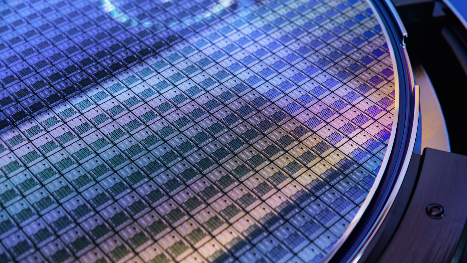
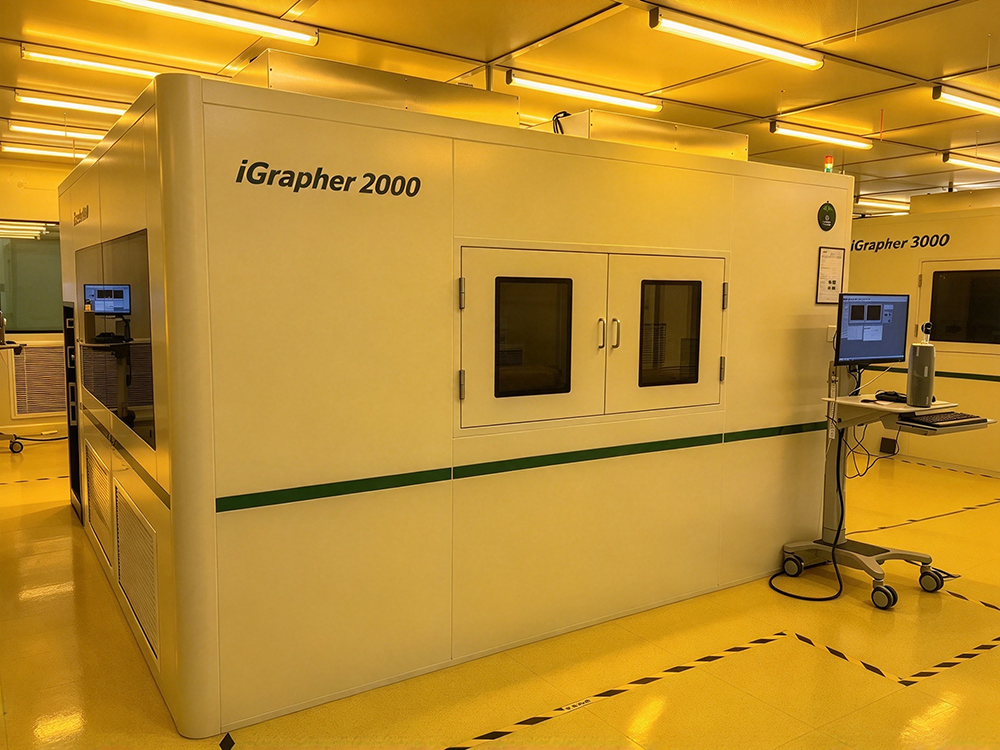
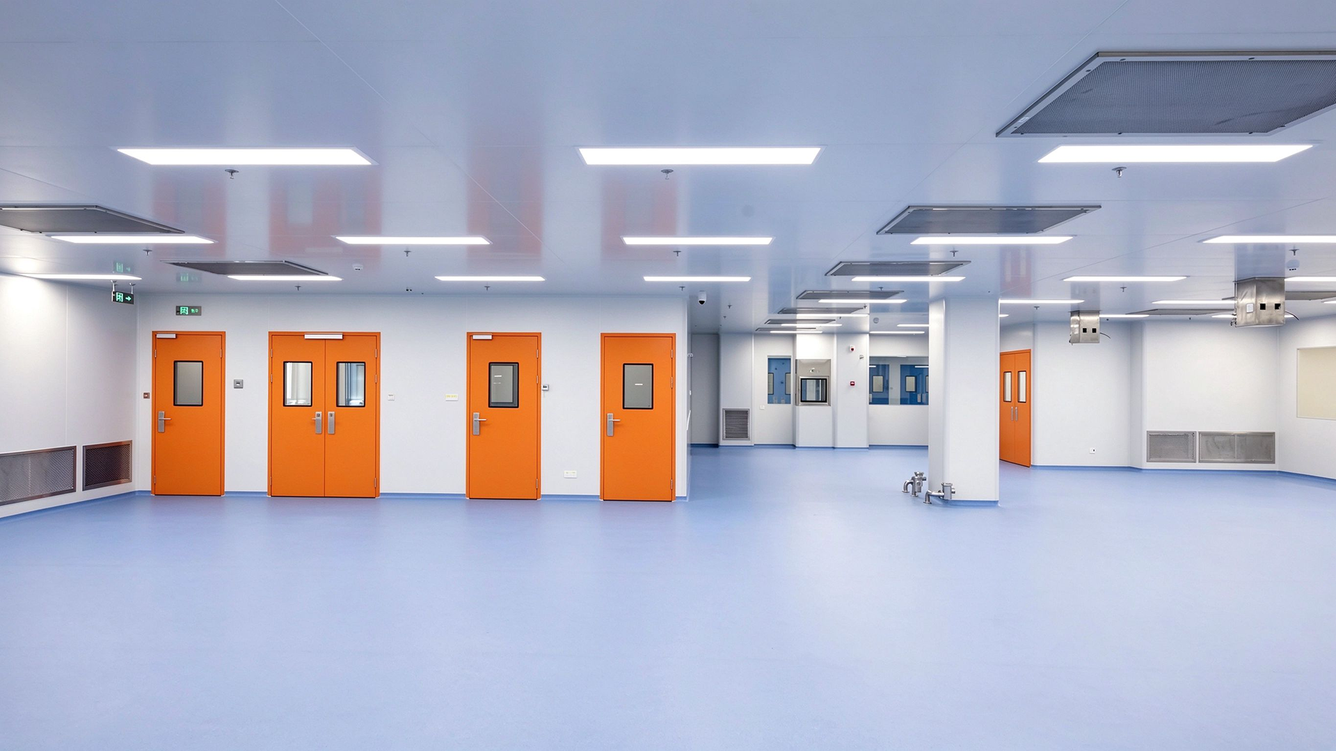
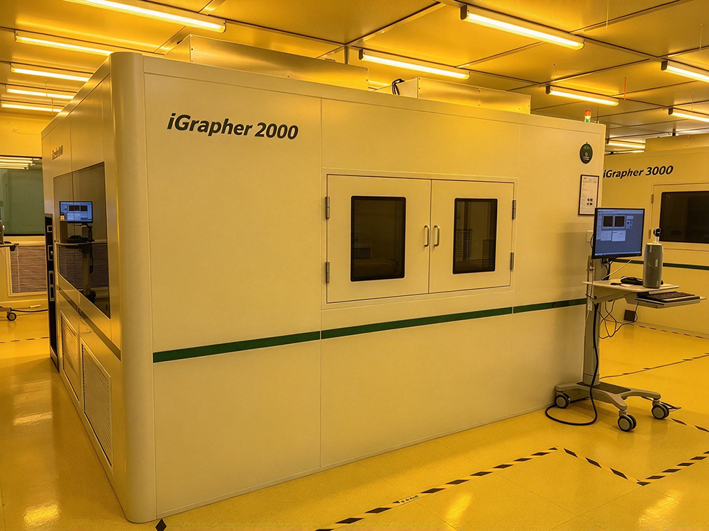
In the nanometer-driven Microelectronics And semiconductor industry, manufacturing environment defines ultimate precision. EasyCube’s high-performance modular cleanrooms are engineered for wafer fabrication and microelectronics assembly, enabling ultra-fast deployment of ultra-clean facilities to keep pace with Moore’s Law. Engineered for stability and precision, our systems deliver superior vibration control, ESD protection and air purity for advanced lithography and etching processes.
EasyCube has redefined modular cleanroom design, manufacturing and construction. Driven by innovation and international standards, we deliver full-cycle EPC and one-stop modular solutions for global clients in complex industrial environments, empowering industrial upgrading and manufacturing reshoring.
Focused on life sciences, pharmaceuticals, semiconductor and advanced manufacturing sectors, we strive to be an industry pioneer and the trusted global partner of choice.
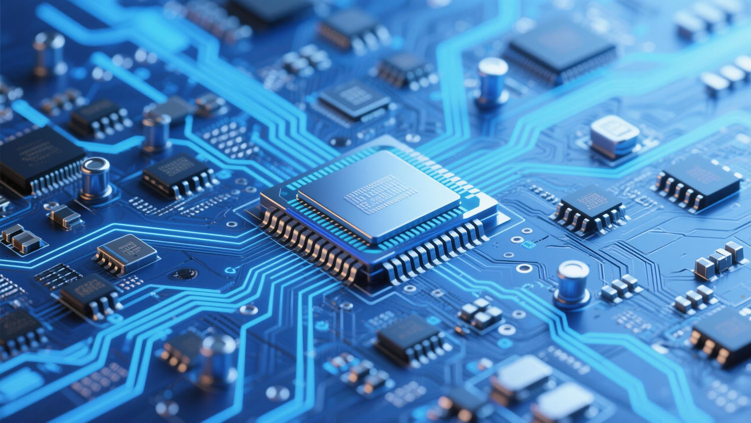
We provide precision-controlled spaces for a comprehensive range of Semiconductor applications, such as:
Ultra-high-purity environments designed for photolithography, etching, and ion implantation, featuring specialized airflow patterns to maintain ISO Class 1–5 cleanliness at the wafer level.
Modular suites for wafer dicing, wire bonding, and flip-chip assembly, providing a cost-effective balance of cleanliness and high-volume throughput.
Specialized environments for the assembly of high-density storage media, where even a single sub-micron particle can cause catastrophic head-to-media failure.
Flexible cleanroom layouts optimized for the production of Micro-Electro-Mechanical Systems, allowing for the integration of specialized wet benches and chemical processing tools.
Isolated, high-stability environments for scanning electron microscopy (SEM) and other diagnostic tools, ensuring environmental noise does not interfere with analytical precision.